(China (Mainland))


Product Summary
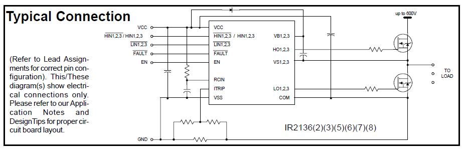
The ir21365 is a high votage, high speed power MOSFET and IGBT driver with three independent high and low side referenced output channels for 3-phase applications. Proprietary HVIC technology of the ir21365 enables ruggedized monolithic construction. Logic inputs are compatible with CMOS or LSTTL outputs, down to 3.3V logic. A current trip function which terminates all six outputs can be derived from an external current sense resistor. An enable function is available to terminate all six outputs simultaneously. An open-drain FAULT signal of the ir21365 is provided to indicate that an overcurrent or undervoltage shutdown has occurred. Overcurrent fault conditions are cleared automatically after a delay programmed externally via an RC network connected to the RCIN input. The ir21365 features a high pulse current buffer stage designed for minimum driver cross-conduction. Propagation delays are matched to simplify use in high frequency applications. The floating channel of the IR2136S can be used to drive N-channel power MOSFETs or IGBTs in the high side configuration which operates up to 600 volts.
Parametrics
ir21365 absolute maximum ratings: (1)VS, High side offset voltage: VB1,2,3 - 25V to VB1,2,3 + 0.3V; (2)VBS, High side floating supply voltage: -0.3V to 625V; (3)VHO, High side floating output voltage: VS1,2,3 - 0.3V to VB1,2,3 + 0.3V; (4)VCC, Low side and logic fixed supply voltage: -0.3V to 25V; (5)VSS, Logic ground: VCC - 25V to VCC + 0.3V; (6)VLO1,2,3 Low side output voltage: -0.3V to VCC + 0.3V; (7)VIN, Input voltage LIN,HIN,ITRIP, EN, RCIN: VSS - 0.3V to lower of (VSS + 15V) or VCC + 0.3V); (8)VFLT, FAULT output voltage: VSS - 0.3 to VCC + 0.3W; (9)dV/dt, Allowable offset voltage slew rate: 50 V/ns; (10)PD, Package power dissipation @ TA ≤ +25℃: 1.6W; (11)RthJA, Thermal resistance, junction to ambient: 78℃/W; (12)TJ, Junction temperature: 150℃; (13)TS, Storage temperature: -55 to 150℃; (14)TL, Lead temperature (soldering, 10 seconds): 300℃.
Features
ir21365 features: (1)Floating channel designed for bootstrap operation Fully operational to +600V, Tolerant to negative transient voltage - dV/dt immune; (2)Gate drive supply range from 10 to 20V; (3)Undervoltage lockout for all channels; (4)Over-current shutdown turns off all six drivers; (5)Independent 3 half-bridge drivers; (6)Matched propagation delay for all channels; (7)Cross-conduction prevention logic; (8)Lowside outputs out of phase with inputs. High side outputs out of phase; (9)3.3V logic compatible; (10)Lower di/dt gate driver for better noise immunity; (11)Externally programmable delay for automatic fault clear; (12)Also available LEAD-FREE.
Diagrams
| Image | Part No | Mfg | Description |  |
Pricing (USD) |
Quantity | ||||||||||||||
|---|---|---|---|---|---|---|---|---|---|---|---|---|---|---|---|---|---|---|---|---|
 |
 IR21365 |
Other |
|
Data Sheet |
Negotiable |
|
||||||||||||||
 |
IR21365JPbF |
International Rectifier |
Power Driver ICs |
Data Sheet |
|
|
||||||||||||||
|
IR21365JTRPBF |
International Rectifier |
Power Driver ICs 3Phs Drvr Sft Trn On Invrt 200ns |
Data Sheet |
|
|
||||||||||||||
|
IR21365SPbF |
International Rectifier |
Power Driver ICs |
Data Sheet |
|
|
||||||||||||||
|
IR21365STRPBF |
International Rectifier |
Power Driver ICs 3Phs Drvr Sft Trn On Invrt 200ns |
Data Sheet |
|
|
||||||||||||||